


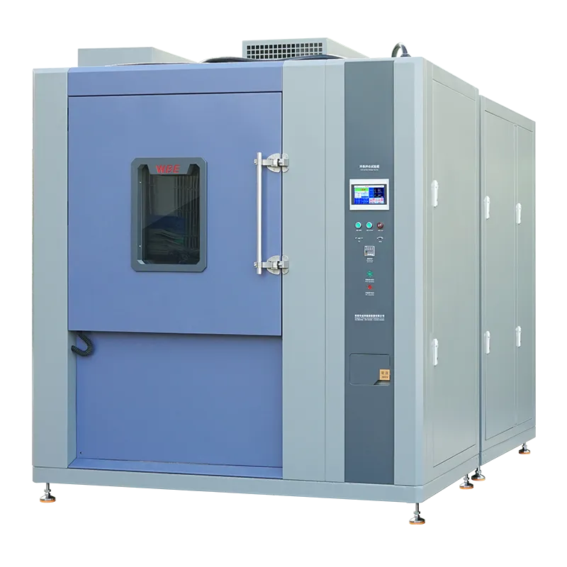
In the rapidly evolving landscape of electronics manufacturing, reliability is the cornerstone of brand reputation and consumer safety. Printed Circuit Boards (PCBs) and their associated solder joints form the nervous system of modern devices, ranging from aerospace navigation systems to medical life-support equipment. These components are frequently subjected to harsh environments where temperatures fluctuate violently. To ensure long-term durability, the use of a thermal shock test chamber has become an indispensable part of the quality assurance process.
Thermal shock testing differs from standard temperature cycling by the speed of the transition. While standard cycling allows for gradual adaptation, a thermal shock environment forces the material to react almost instantaneously to extreme temperature differentials. This guide explores the deep technical applications of this testing method, focusing on how it uncovers hidden vulnerabilities in PCB substrates and solder interconnections.
The Mechanics of Thermal Shock in Electronics
The fundamental principle behind the thermal shock test chamber is the rapid transfer of energy. When a PCB is moved from a hot zone (often up to 150 degrees Celsius) to a cold zone (as low as -65 degrees Celsius) within seconds, the various materials within the board expand and contract at different rates. This phenomenon is known as the Coefficient of Thermal Expansion (CTE) mismatch.
Most PCBs are composite structures made of fiberglass-reinforced epoxy (FR-4), copper foil, and various plating materials. The epoxy resin typically has a much higher CTE than the copper traces and vias. Under the stress of a thermal shock test chamber, these internal stresses are magnified. If the bond between the copper and the resin is weak, or if the plating in the through-holes is brittle, the rapid transition will cause physical separation or cracking.
Testing usually involves two or three zones. In a two-zone configuration, the basket containing the samples moves vertically or horizontally between high and low temperature compartments. In a three-zone setup, an ambient temperature dwell is included. For PCB and solder joint validation, the two-zone liquid-to-liquid or air-to-air method is most common, as it provides the steepest temperature gradients required to trigger infant mortality failures in poorly manufactured lots.
Critical PCB Failure Modes Detected
One of the most catastrophic failures in PCB assemblies is delamination. This is the separation of the internal layers of the board. During the rapid cooling phase in a thermal shock test chamber, trapped moisture or volatiles within the epoxy can exert pressure, leading to "popcorning" or layer separation. Without such rigorous testing, these defects might remain hidden until the product is in the hands of the end-user, leading to costly recalls.
Plated Through-Holes (PTH) and Vias are also highly susceptible. The copper plating within a via acts like a rivet. As the PCB expands in the Z-axis during the heat phase, it pulls on the copper barrel. In the cold phase, it compresses. Repeated cycles in a thermal shock test chamber cause fatigue in the copper, eventually leading to barrel cracking or "corner cracks" at the junction of the via and the surface pad.
Inner-layer Interconnect Stress: Identifying separation between internal copper traces and via walls.
Solder Mask Cracking: Evaluating the brittleness of protective coatings under extreme contraction.
Resin Recession: Observing the shrinkage of the dielectric material away from the hole walls.
Solder Joint Integrity and Fatigue Analysis
Solder joints serve a dual purpose: they provide electrical connectivity and mechanical support. Modern lead-free solders, such as SAC305, are more brittle than traditional tin-lead versions. This makes them particularly vulnerable to thermal fatigue. When an electronic assembly is placed in a thermal shock test chamber, the solder joint is caught between the expanding component package and the expanding PCB substrate.
Because the component (often made of ceramic or silicon) and the PCB (FR-4) have vastly different CTE values, the solder joint must absorb the resulting shear strain. Over many cycles, this strain leads to the formation of micro-cracks within the solder grain structure. These cracks typically propagate along the Intermetallic Compound (IMC) layer, eventually causing a complete open circuit.
Advanced analysis post-testing involves cross-sectioning and scanning electron microscopy (SEM) to determine the health of the IMC. A thermal shock test chamber allows engineers to accelerate this aging process. What would normally take five years of field use can be simulated in a few hundred cycles, allowing for rapid design iterations and material selection for harsh environment applications.
Strategic Testing Advice and Standards
To achieve meaningful results, testing must align with global standards such as IPC-9701 or MIL-STD-810G. These standards define the required dwell times at temperature extremes and the number of cycles needed for qualification. It is generally advised that the dwell time should be long enough for the internal temperature of the test specimen to stabilize, typically between 15 to 30 minutes for standard PCBs.
Furthermore, monitoring "in-situ" or in real-time is highly recommended. By connecting the PCB to a data logger while it is inside the thermal shock test chamber, engineers can detect intermittent failures that only occur at temperature peaks. These "glitches" often disappear once the board returns to room temperature, making them impossible to find through post-test inspection alone.
Choosing the right equipment is equally critical. A chamber with high airflow velocity ensures that the heat transfer coefficient is maximized, leading to the fastest possible transition rates on the product surface. This mimics real-world "worst-case scenarios," such as an automotive ECU being started in sub-zero temperatures after sitting in a hot engine bay.
The WBE Advantage in Environmental Testing
As a leader in the environmental testing industry, WBE (Guangdong Yuanyao Test Equipment Co., Ltd.) provides cutting-edge solutions for complex reliability challenges. Our expertise extends beyond mere manufacturing; we provide integrated testing solutions that help companies validate their most sensitive electronic components. We understand that the precision of a thermal shock test chamber can make the difference between a successful product launch and a catastrophic field failure.
At WBE, our product lineup is designed for versatility and accuracy. We offer a variety of specialized equipment including:
Thermal Shock Solutions
High-performance two-slot thermal shock test chamber and three-slot models for rigorous stress testing.
Climatic Chambers
Sophisticated high and low temperature humidity test chambers for steady-state environmental simulation.
Mechanical Testing
Precision bond tester machines and push-pull testers for solder strength verification.
Specialized Aging
Advanced HAST aging test chambers for accelerated life testing of semiconductors.
Our commitment to quality is reflected in our robust design and user-friendly control systems. Whether you are testing small-scale semiconductor packages or large-scale automotive assemblies, our comprehensive range of environmental testing equipment ensures that your products meet the highest international standards.
Conclusion
The role of a thermal shock test chamber in PCB and solder joint testing cannot be overstated. By subjecting electronic assemblies to the most punishing thermal gradients, manufacturers can identify and rectify design flaws long before they reach the market. From detecting delamination in high-layer-count boards to validating the fatigue life of microscopic solder balls in BGA packages, thermal shock testing is the ultimate filter for quality.
Partnering with an experienced equipment manufacturer like WBE ensures that your testing lab is equipped with the precision, reliability, and technical support needed to navigate the complexities of modern electronics validation. As devices become smaller and environments become more extreme, the investment in high-quality testing equipment remains the best insurance policy for any technology-driven enterprise.
FAQ: Thermal Shock Testing Insights
Q1: What is the primary function of a thermal shock test chamber in PCB validation?
The primary function is to induce rapid thermal expansion and contraction in the PCB's composite materials. This stress reveals weaknesses in the bond between layers (delamination) and tests the integrity of copper-plated vias, ensuring the board can withstand extreme environmental transitions without electrical failure.
Q2: How many cycles should be performed in a thermal shock test chamber for solder joint reliability?
Depending on the industry standard (such as IPC-9701), the number of cycles can range from 100 for consumer electronics to over 1,000 for aerospace or automotive applications. The goal is to reach the point of thermal fatigue to determine the expected service life of the solder interconnection.
Q3: Which industries rely most on a thermal shock test chamber for product safety?
The automotive, aerospace, defense, and medical device industries are the primary users. Any sector where electronic failure could lead to loss of life or significant financial damage utilizes these chambers to guarantee that their systems operate reliably in fluctuating temperatures.
Q4: What are the key maintenance steps for a high-performance thermal shock test chamber?
Routine maintenance includes checking the refrigeration system's pressure, calibrating temperature sensors for accuracy, inspecting the basket transport mechanism for smooth operation, and ensuring the chamber door seals are airtight to prevent frost buildup and energy loss.
Q5: How does a thermal shock test chamber differ from a standard temperature cycling chamber?
The core difference is the "ramp rate" or transition speed. A standard chamber changes temperature gradually (e.g., 5-10°C per minute), whereas a thermal shock chamber moves the product between pre-heated and pre-cooled zones almost instantly, achieving transition rates that can exceed 30°C per minute on the product surface.
Ready to Enhance Your Product Reliability?
Contact WBE today to find the perfect testing solution for your laboratory.